



The most fought-over step in building an AI chip is no longer the chip. It is the package the chip goes into. In a report published on November 6, Reuters described advanced chip packaging, a stage of manufacturing the industry barely used to think about, as a critical bottleneck in turning out the world’s most powerful processors. Demand for AI chips now outstrips the world’s packaging capacity, and companies from Nvidia and AMD to smaller firms across Taiwan are spending billions of dollars to expand it.
What chip packaging actually is
For most of computing history, packaging was the last and least glamorous step of making a chip. Once the circuitry was printed onto silicon, the chip was sealed in a protective shell and given the metal connections that attach it to a circuit board. As former Intel chief executive Pat Gelsinger, now a partner at Playground Global, told reporters in Taipei: “Packaging was always that thing that you just didn’t worry about.”
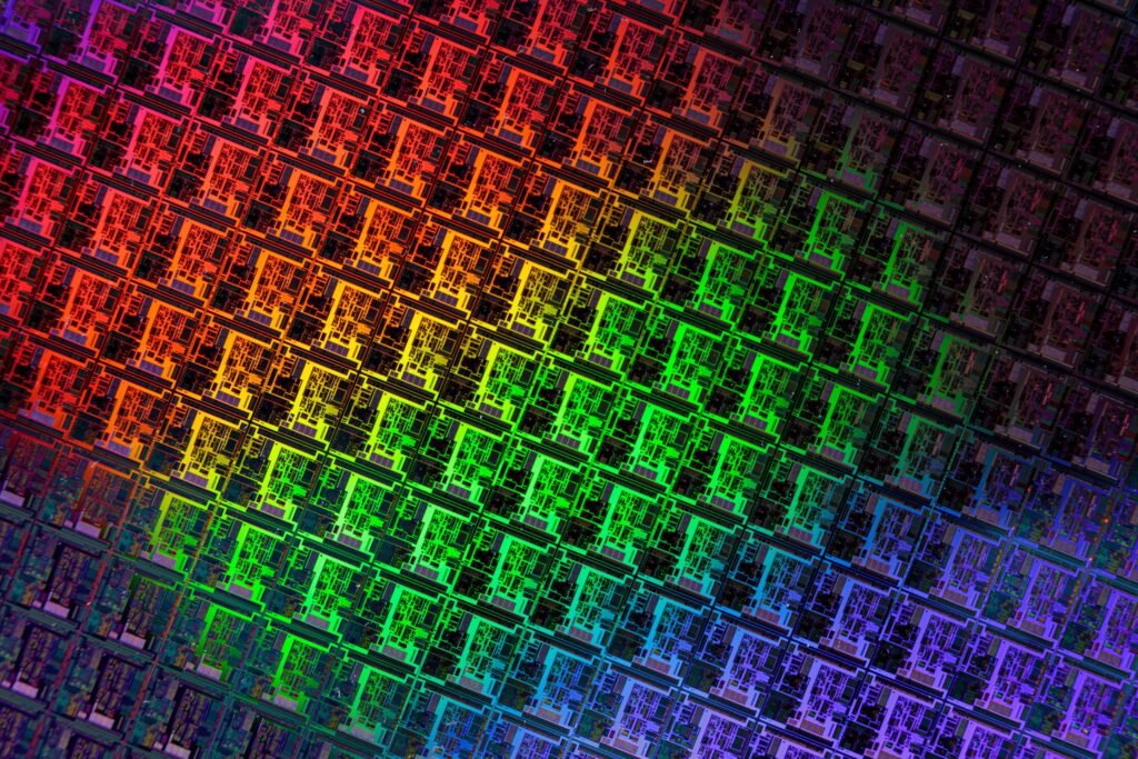
Advanced packaging is a different job entirely. Instead of housing a single chip, it joins several separate pieces of silicon, a processor here, memory chips there, sometimes other parts as well, into one package where they work together as a single system. Done well, the combined unit runs far faster than the same chips could sitting apart on a board, talking across longer, slower connections.
Why AI made packaging the main event
Two forces pushed packaging to the center of the industry. The first is physics. For decades, chips got faster mainly by shrinking their transistors, the tiny switches inside them. Reuters notes that those gains have become harder and costlier to win, so designers increasingly win speed from how chips are combined, not from the chips alone.
The second force is how AI actually works. Training and running an AI model means moving enormous amounts of data between the processor and the memory, back and forth, billions of times. If the memory sits far away, the processor spends its time waiting. Advanced packaging solves this by placing stacks of high bandwidth memory, the fast memory known as HBM, directly beside the processor, wired together over very short distances. The result is that the package is no longer a shell around the product. It is part of what makes the product fast.
CoWoS, the package everyone is queuing for
The technology at the center of the race is called CoWoS, short for chip-on-wafer-on-substrate, and it belongs to TSMC, the world’s largest contract chipmaker. The processor and memory dies are first joined side by side on a silicon wafer that is dense with wiring, so the pieces can exchange data at very high speed. That assembly is then mounted on a substrate, the base that connects it to the rest of the computer.
TSMC dominates this technology, and nearly everyone who matters in AI depends on it. Reuters reports that CoWoS is widely used by Nvidia, AMD and Broadcom, as well as by cloud companies building their own AI chips. The problem is quantity: TSMC’s packaging capacity is limited, and that limit has become the industry’s choke point, pushing chip designers to hunt for second sources.
Billions are now chasing capacity
The clearest sign of how tight supply has become is what Nvidia is reportedly doing about it. According to an industry executive familiar with the matter, Nvidia is providing billions of dollars in financing to expand CoWoS packaging capacity at Siliconware Precision Industries, known as SPIL, a unit of Taiwan’s ASE Technology. The money would pay for new factory space and equipment, and the scale of the support had not been reported before. Nvidia did not respond to a request for comment, and ASE said it does not comment on market rumors involving its customers. A customer paying to build a supplier’s factory is an unusual move, and it reflects Nvidia’s position at the center of the AI build-out, the same position that made its shares the heaviest weight in the AI selloff that hit chip stocks this week.
AMD is spending heavily too. It has unveiled investments of more than $10 billion across Taiwan’s semiconductor industry, including partnerships with ASE, SPIL and Powertech on advanced packaging. “I think CoWoS and advanced packaging are super important for our high-performance computing going forward,” AMD chief executive Lisa Su told Reuters in Taipei in October. “TSMC has been an incredible partner in advanced packaging, and we’re going to continue to do more together. And yes, we do need more capacity overall.”
Powertech Technology, or PTI, is betting on a different route around the bottleneck: panel-level packaging, which uses larger rectangular panels instead of round wafers. Panels fit more of today’s large AI chips in each run and waste less material. “Everyone is looking for a solution outside TSMC,” PTI chairman D K Tsai told reporters. “They don’t want to rely entirely on TSMC.” PTI is working with AMD and Broadcom on the technology, and it plans to invest $400 million in an advanced packaging joint venture with Broadcom in Singapore, where production could begin in 2028. “The most important thing right now is capacity,” said PTI senior vice president Jim Lin.
TSMC is not standing still. It is developing its own panel-based technology, called CoPoS, and said in April that it had built a pilot line, with production expected to begin within a couple of years, though CoWoS remains its main AI packaging technology. The equipment makers who supply the factories are rushing in too. Advanced packaging is growing much faster than the market for chip-making gear, Tokyo Electron Taiwan president Seiji Nakama told Reuters, and Applied Materials vice president Sree Kesapragada expects significant growth within three to five years. “It’s near-term,” he said. “It’s not like, 10 years, 15 years off.”
Why the package now decides who gets AI chips
The numbers explain why so much money is moving. Gelsinger estimated that advanced packaging could eventually account for as much as half the value of a chip product, because a modern processor can integrate 10 or more individual chips, sometimes as many as 20. Research firm Yole Group forecasts that revenue from advanced packaging will overtake revenue from traditional packaging for the first time in 2026, with capital spending on the technology expected to near $28 billion.
The practical meaning is simple. A company can design a brilliant AI processor and have its silicon printed on schedule, and still ship nothing until there is packaging capacity to finish it. The queue for that capacity now decides whose AI chips reach data centers and whose wait another quarter. That is why the industry’s biggest customers are suddenly funding factories they do not own, and why a step nobody used to worry about has become the one everyone is watching. We will keep following it in our Technology coverage.
Sources: Reuters, “AI boom turns chip packaging into the next battleground for semiconductors,” November 6, 2026, reporting by Wen-Yee Lee in Taipei, based on interviews with more than a dozen industry executives and analysts; forecast figures from Yole Group as reported by Reuters.